
Recent Market Analysis of Atomic Layer Etching Equipment by The Business Research Company, Emphasizing Upcoming Industry

The Business Research Company
Atomic Layer Etching Equipment
The Business Research Company’s Atomic Layer Etching Equipment Global Market Report 2026 – Market Size, Trends, And Forecast 2026-2035
LONDON, GREATER LONDON , UNITED KINGDOM, October 15, 2026 /EINPresswire.com/ -- The atomic layer etching equipment market is gaining remarkable traction as semiconductor technology advances rapidly. With the increasing complexity of devices and demand for precision manufacturing, this sector is poised for significant growth. Below, we explore the current market size, the main drivers behind its expansion, leading regional players, and the trends shaping the future of atomic layer etching equipment.
Strong Expansion and Future Outlook for the Atomic Layer Etching Equipment Market
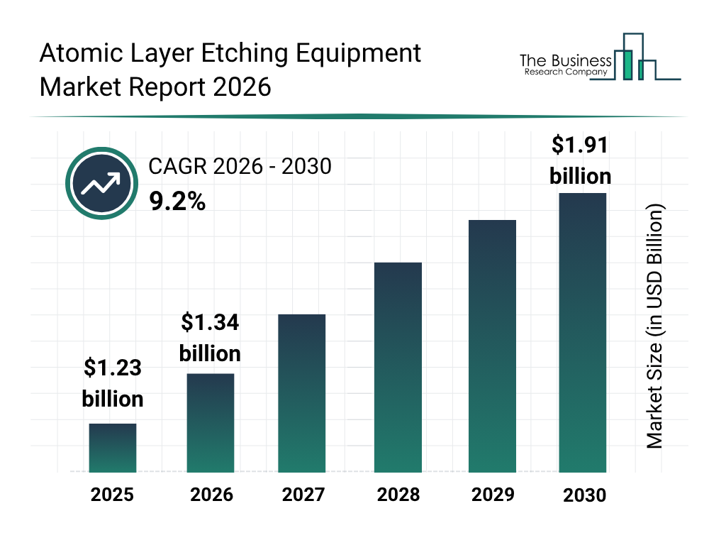
The atomic layer etching equipment market has seen substantial growth in recent years. It is projected to increase from $1.23 billion in 2025 to $1.34 billion in 2026, reflecting a compound annual growth rate (CAGR) of 9.5%. This historical growth is largely driven by rising demand for sophisticated semiconductor devices, a shift toward smaller semiconductor geometries, the growing necessity for precise wafer material removal, an increase in semiconductor manufacturing capacity, and the broader adoption of advanced patterning processes.
Download a free sample of the atomic layer etching equipment market report:
https://www.thebusinessresearchcompany.com/sample_request?id=85462577&type=smp&name=Atomic%20Layer%20Etching%20Equipment%20Market%20Report%202026&utm_source=EINPresswire&utm_medium=Paid&utm_campaign=Oct_PR
Looking ahead, the market is expected to continue its robust growth trajectory, reaching $1.91 billion by 2030, with a CAGR of 9.2%. This forecasted expansion is fueled by the increasing need for atomic-scale process control, wider adoption of advanced logic and memory devices, a growing requirement for high-aspect-ratio etching, heightened demand for selective material removal, and the production of next-generation semiconductor architectures. Key trends shaping this period include broader implementation of atomic-level wafer processing, growing interest in high-precision semiconductor etching, increased use of self-limiting etching techniques, and an intensified focus on selective, damage-free material removal.
Understanding the Role and Function of Atomic Layer Etching Equipment
Atomic layer etching (ALE) equipment plays a crucial role in semiconductor manufacturing by enabling the removal of ultra-thin material layers from wafers with atomic-scale accuracy. This process relies on tightly controlled, self-limiting chemical reactions to ensure precision. ALE equips manufacturers with the capability to achieve intricate patterning and fabrication essential for advanced semiconductor devices.
View the full atomic layer etching equipment market report:
https://www.thebusinessresearchcompany.com/report/atomic-layer-etching-equipment-market-report?utm_source=EINPresswire&utm_medium=Paid&utm_campaign=Oct_PR
Investment in Semiconductor Fabrication Facilities Boosts Market Growth
One of the primary forces propelling the atomic layer etching equipment market is the increasing investment in semiconductor fabrication facilities. These specialized plants produce integrated circuits and semiconductor devices through controlled processes like deposition, lithography, etching, doping, and packaging. The surge in investment is driven by rising demand for advanced semiconductor chips used in applications such as artificial intelligence, high-performance computing, 5G networks, electric vehicles, and consumer electronics.
As semiconductor fabs expand and new ones emerge, there is a growing need for advanced etching technologies that deliver atomic-level precision, high selectivity, and meticulous process control to support manufacturing at cutting-edge technology nodes. For example, in August 2024, the U.S. Department of Commerce reported over $30 billion in proposed private-sector investments under the CHIPS and Science Act. These funds support 23 projects across 15 states, including 16 new semiconductor manufacturing plants expected to generate more than 115,000 manufacturing and construction jobs. This surge in fab investments is a significant factor driving the atomic layer etching equipment market forward.
North America Leads, While Asia-Pacific Emerges as a Rapid Growth Frontier
In 2025, North America held the largest share of the atomic layer etching equipment market. However, the Asia-Pacific region is forecasted to experience the fastest growth over the coming years. The market report covers a broad array of geographical regions, including Asia-Pacific, South East Asia, Western Europe, Eastern Europe, North America, South America, the Middle East, and Africa, providing a comprehensive view of global market dynamics.
Our latest 2026 market reports provide expanded strategic and visual intelligence with market attractiveness scoring and analysis, total addressable market (TAM) analysis, company scoring matrix graphics and tables, Excel-based forecasting dashboards, market hotspots infographics, key technologies and future trend analysis, together with updated graphics and tables.
Speak With Our Expert:
Saumya Sahay
Americas +1 310-496-7795
Asia +44 7882 955267 & +91 8897263534
Europe +44 7882 955267
Email: marketing@tbrc.info
The Business Research Company - www.thebusinessresearchcompany.com
Follow Us On:
• LinkedIn: https://in.linkedin.com/company/the-business-research-company.
Oliver Guirdham
The Business Research Company
+44 7882 955267
info@tbrc.info
Visit us on social media:
LinkedIn
Facebook
X
Legal Disclaimer:
EIN Presswire provides this news content "as is" without warranty of any kind. We do not accept any responsibility or liability for the accuracy, content, images, videos, licenses, completeness, legality, or reliability of the information contained in this article. If you have any complaints or copyright issues related to this article, kindly contact the author above.
